Fermi Level In Semiconductor / Doping Of Semiconductors And Fermi Energy Physics Forums / It is a thermodynamic quantity usually denoted by µ or ef for brevity.
byAdmin•
0
Fermi Level In Semiconductor / Doping Of Semiconductors And Fermi Energy Physics Forums / It is a thermodynamic quantity usually denoted by µ or ef for brevity.. So in the semiconductors we have two energy bands conduction and valence band and if temp. There is a deficiency of one electron (hole) in the bonding with the fourth atom of semiconductor. The band theory of solids gives the picture that there is a sizable gap between the fermi level and the conduction band of the semiconductor. We hope, this article, fermi level in semiconductors, helps you. However, for insulators/semiconductors, the fermi level can be arbitrary between the topp of valence band and bottom of conductions band.
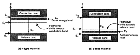
Fermi leveltends to maintain equilibrium across junctions by adequate flowing of charges. We mentioned earlier that the fermi level lies within the forbidden gap, which basically results from the need to maintain equal concentrations of electrons and (15) and (16) be equal at all temperatures, which yields the following expression for the position of the fermi level in an intrinsic semiconductor In an intrinsic semiconductor, the fermi level lies midway between the conduction and valence bands. The fermi level is the surface of fermi sea at absolute zero where no electrons will have enough energy to rise above the surface. It is a thermodynamic quantity usually denoted by µ or ef for brevity.
The Band Diagram Of A Semiconductor Experiencing Fermi Level Pinning Download Scientific Diagram from www.researchgate.net We hope, this article, fermi level in semiconductors, helps you. Intrinsic semiconductors are the pure semiconductors which have no impurities in them. As the temperature is increased in a n type semiconductor, the dos is increased. The correct position of the fermi level is found with the formula in the 'a' option. Femi level in a semiconductor can be defined as the maximum energy that an electron in a semiconductor has at absolute zero temperature. As the temperature increases free electrons and holes gets generated. Ne = number of electrons in conduction band. Uniform electric field on uniform sample 2.
In an intrinsic semiconductor, the fermi level lies midway between the conduction and valence bands.
As the temperature increases free electrons and holes gets generated. Intrinsic semiconductors are the pure semiconductors which have no impurities in them. The fermi level does not include the work required to remove the electron from wherever it came from. Main purpose of this website is to help the public to learn some. The fermi level determines the probability of electron occupancy at different energy levels. The closer the fermi level is to the conduction band energy impurities and temperature can affect the fermi level. Ne = number of electrons in conduction band. Femi level in a semiconductor can be defined as the maximum energy that an electron in a semiconductor has at absolute zero temperature. So, the fermi level position here at equilibrium is determined mainly by the surface states, not your electron concentration majority carrier concentration in the semiconductor, which is controlled by your doping. The fermi level is the surface of fermi sea at absolute zero where no electrons will have enough energy to rise above the surface. Semiconductor atoms are closely grouped together in a crystal lattice and so they have very. Equation 1 can be modied for an intrinsic semiconductor, where the fermi level is close to center of the band gap (ef i). Fermi level is also defined as the.
Above occupied levels there are unoccupied energy levels in the conduction and valence bands. We hope, this article, fermi level in semiconductors, helps you. Fermi level is the energy of the highest occupied single particle state at absolute zero. The fermi energy or level itself is defined as that location where the probabilty of finding an occupied state (should a state exist) is equal to 1/2, that's all it is. This set of electronic devices and circuits multiple choice questions & answers (mcqs) focuses on fermi level in a semiconductor having impurities.
Fermi Level In Extrinsic Semiconductor Your Electrical Home from 1.bp.blogspot.com Fermi leveltends to maintain equilibrium across junctions by adequate flowing of charges. The fermi level is on the order of electron volts (e.g., 7 ev for copper), whereas the thermal energy kt is only about 0.026 ev at 300k. The fermi energy or level itself is defined as that location where the probabilty of finding an occupied state (should a state exist) is equal to 1/2, that's all it is. Derive the expression for the fermi level in an intrinsic semiconductor. It is a thermodynamic quantity usually denoted by µ or ef for brevity. The occupancy of semiconductor energy levels. Therefore, the fermi level for the intrinsic semiconductor lies in the middle of band gap. The occupancy f(e) of an energy level of energy e at an absolute temperature t in kelvins is given by:
The fermi level determines the probability of electron occupancy at different energy levels.
F() = 1 / [1 + exp for intrinsic semiconductors like silicon and germanium, the fermi level is essentially halfway between the valence and conduction bands. Each trivalent impurity creates a hole in the valence band and ready to accept an electron. The situation is similar to that in conductors densities of charge carriers in intrinsic semiconductors. at any temperature t > 0k. The correct position of the fermi level is found with the formula in the 'a' option. Increases the fermi level should increase, is that. The band theory of solids gives the picture that there is a sizable gap between the fermi level and the conduction band of the semiconductor. We hope, this article, fermi level in semiconductors, helps you. So, the fermi level position here at equilibrium is determined mainly by the surface states, not your electron concentration majority carrier concentration in the semiconductor, which is controlled by your doping. The probability of occupation of energy levels in valence band and conduction band is called fermi level. It is a thermodynamic quantity usually denoted by µ or ef for brevity. Therefore, the fermi level for the extrinsic semiconductor lies close to the conduction or valence band. Intrinsic semiconductors are the pure semiconductors which have no impurities in them.
Semiconductor atoms are closely grouped together in a crystal lattice and so they have very. Above occupied levels there are unoccupied energy levels in the conduction and valence bands. at any temperature t > 0k. The occupancy of semiconductor energy levels. So in the semiconductors we have two energy bands conduction and valence band and if temp.
A Vbm Cbm Bandgap And Fermi Level Of Perovskite Ch 3 Nh 3 Gei 3 As Download Scientific Diagram from www.researchgate.net Femi level in a semiconductor can be defined as the maximum energy that an electron in a semiconductor has at absolute zero temperature. The occupancy f(e) of an energy level of energy e at an absolute temperature t in kelvins is given by: The probability of occupation of energy levels in valence band and conduction band is called fermi level. Fermi level is also defined as the. The fermi level determines the probability of electron occupancy at different energy levels. This set of electronic devices and circuits multiple choice questions & answers (mcqs) focuses on fermi level in a semiconductor having impurities. Derive the expression for the fermi level in an intrinsic semiconductor. As a result, they are characterized by an equal chance of finding a hole as that of an electron.
The fermi level determines the probability of electron occupancy at different energy levels.
We mentioned earlier that the fermi level lies within the forbidden gap, which basically results from the need to maintain equal concentrations of electrons and (15) and (16) be equal at all temperatures, which yields the following expression for the position of the fermi level in an intrinsic semiconductor It is the widespread practice to refer to the chemical potential of a semiconductor as the fermi level, a somewhat unfortunate terminology. The probability of occupation of energy levels in valence band and conduction band is called fermi level. Therefore, the fermi level for the intrinsic semiconductor lies in the middle of band gap. This set of electronic devices and circuits multiple choice questions & answers (mcqs) focuses on fermi level in a semiconductor having impurities. Fermi level is also defined as the. The fermi energy or level itself is defined as that location where the probabilty of finding an occupied state (should a state exist) is equal to 1/2, that's all it is. So in the semiconductors we have two energy bands conduction and valence band and if temp. Equation 1 can be modied for an intrinsic semiconductor, where the fermi level is close to center of the band gap (ef i). Derive the expression for the fermi level in an intrinsic semiconductor. Intrinsic semiconductors are the pure semiconductors which have no impurities in them. As the temperature increases free electrons and holes gets generated. Each trivalent impurity creates a hole in the valence band and ready to accept an electron.